Evil Eye Tech Experiment
This wasn’t so much a useful project as it was an experiment with some technologies I’ve wanted to play with.
- Capacitive Touch sensing
- LED Multiplexing
- PCB Art
I thought I could combine them to make a stylized Turkish “Evil Eye.” It would:
- Sense when you were near it (Capacitive Touch)
- (near, not touch, was the goal)
- Make a pretty animation (LED multiplexing)
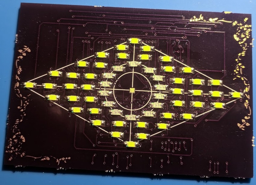
- Look good even when not blinking (PCB art)
Further, I wanted it to be battery powered and survive for years.
The current implementation is estimated to live for 3.8 years on two AAA batteries leveraging deep sleep on the microcontroller and a low-power state on the capacitive touch sensor. Checks for touch 2 times/sec.
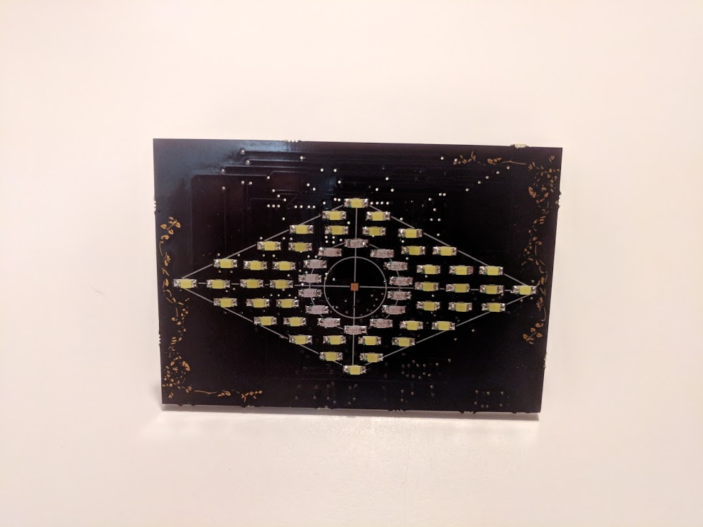
Final look:
Technologies
Microcontroller
Power consumption (microamps)
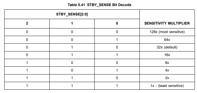
Capacitive Touch sensor (CAP1188)
PCB Fabrication
SMD Parts/Soldering
Research and Build
Capacitive Touch
I had known about the Capacitive Touch sensor from back when I did my synthesizer (link), it was the module behind the piano keyboard interface. However, I hadn’t used it directly.
As noted, I wanted to ramp up sensitivity so that simply being near an exposed lead would trigger an event. I was able to be 1/2″ away during breadboard testing.
In the final PCB, touch sensing works, but proximity sensing doesn’t, even when I ramp up the sensitivity to the max.
I believe the size of the exposed pad was too small, as I was able to make it work subsequently in other configurations.
CAP1188 Datasheet (link)
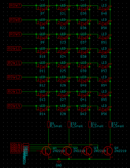
LED Multiplexing
The microcontroller I use (Atmega328P) has 28 pins total, but what if I want to control many more LEDs (light emitting diodes)?
A form of multiplexing can be used, where you construct a matrix of rows and columns. You scan top to bottom, row by row, illuminating only LEDs on that row before moving on.
You do this quickly enough that the human eye perceives a constant illumination (persistence of vision).
The number of rows and columns matters in a number of ways:
- If you have a lot of rows, that means your LED “on time” is 1/<rowCount>
- The more columns you have, the more current you spend when all LEDs are illuminated on a row
The number of usable microcontroller pins (for example, 12), the optimal split is a 6×6 matrix, getting you a maximum of 36 controllable LEDs.
If you want many rows instead, a matrix of 10 rows and 2 columns gets you 20 controllable LEDs. Much worse, but tradeoffs may make this desirable.
In my case, I had a 14×4 matrix to avoid illuminating too many LEDs at a time, as I had concerns around the microcontroller’s ability to deliver enough current.
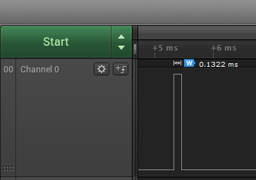
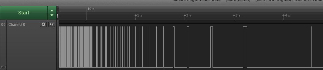
I drove the rows quickly, at ~133 microseconds per row.
Electrically, getting a given LED to illuminate entails:
- Provide voltage on the LED’s row
- Enable that resulting current to get to GND via the LED, by opening a transistor on that LED’s column
Multiplexing and Animation
Driving the multiplexing is software which:
- Has asynchronous code firing at x interval to update each next row
- Consults an in-memory table of on/off values to know how to light each row
The above multiplexer library runs on its own.
Other bits of code drive the animations, like turning on the iris of the eye, or drawing lines. That is done by modifying the multiplexer’s table of on/off values.
The shimmering effect is actually a trick, where I simply slowly lower the rate of row-drawing, leaving some LEDs on longer than others. Given the dispersed placement of LEDs on the board, it looks cool.
Scope shows the ~132-microsecond row duration stepping back to 80 milliseconds gradually.
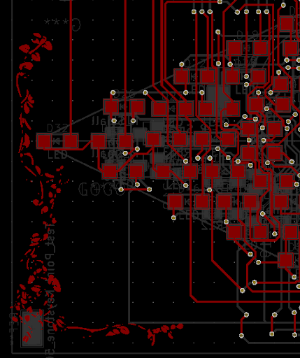
PCB Art
In PCB layout/fabrication, most of the time you’re putting down “footprints” of components. The squares and lines seen on a PCB are the wires you want to connect.
However, the tolerances offered by PCB fabrication houses is incredible, down to 0.006 inches (6 mills).
The specification of copper on a board isn’t in terms of squares and wires, it’s really a mask of types which ultimately dictates what copper “remains” on the board after etching.
The ivy art below is simply a specification to not remove the copper, in a shape which looks like ivy.
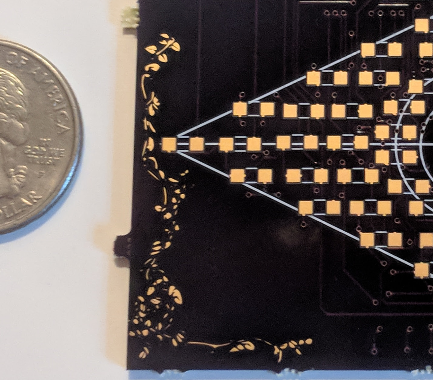
Here you can see (in red) the areas of copper to not remove. The ivy is no different than normal traces and pads.
KiCad (the PCB layout program) provides tools for importing images and converting them into forms suitable for placing on a PCB.
For more complex graphics like on the back of the PCB, I used Inkscape (vector graphics) to create, and external-to-KiCad libraries to convert into a footprint file, which gets loaded into KiCad a different way.
Github
Main file here (link)
Supporting libraries under here (link)
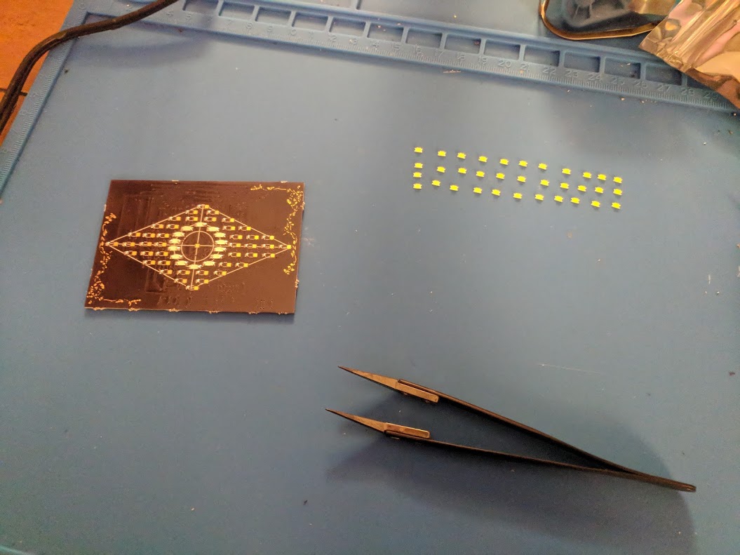
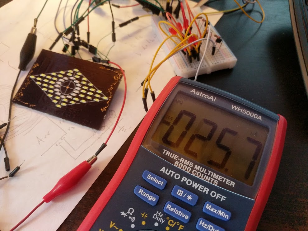
Build Photos and Demo Video
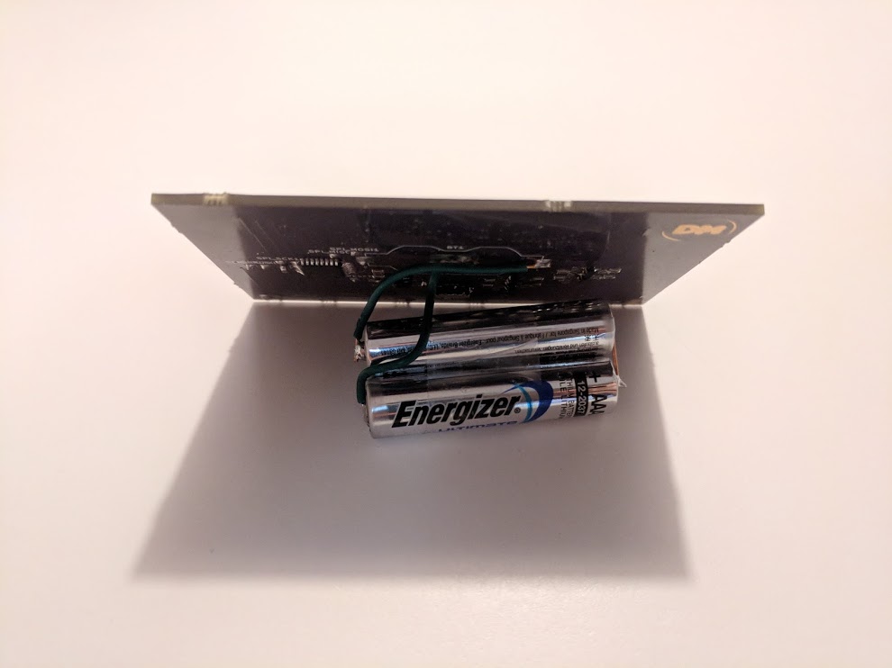
Not a super interesting build! Mostly SMD stuff, plus some ugly wires needed for programming and debugging (eventually taken off of course).
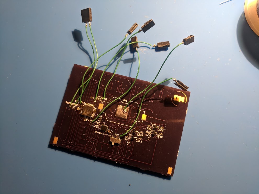
The batteries are soldered directly on, and also act as a stand.
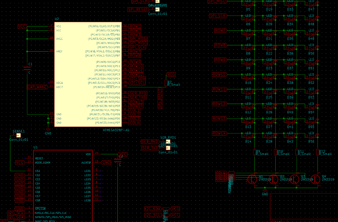
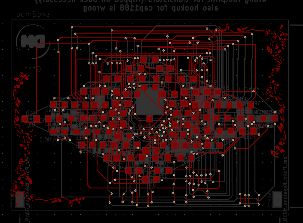
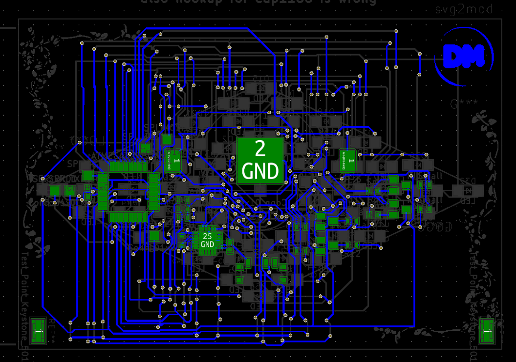
Here are the KiCad circuit and PCB front/back layouts. Routing the LEDs was such a pain.
And the animation again: